Hello dear interwebs,
I just found this blog post that I wrote in 2013… Never finished it, never published it… I’ve updated it slightly (in blue) and then finished writing it so I can finally publish it 6 years later… here it goes :
I was recently thinking about how computers work and I know a lot of you reading me would enjoy knowing more about the details of it, so I decided to write another educational post (kind of like the ECDSA post a few months years ago).
Once more, I need to write a disclaimer saying that this is a relatively simple explanation, I will try to make it easy to understand, but it means there might be some inaccuracies, or incomplete information, so don’t be surprised if you see something wrong, just let me know, it might be my mistake, or it might have been on purpose for the sake of simplicity.
Binary data
First, let’s start with the basics. Many of you will know what binary data is and how it works, but I don’t think everyone does, so I’ll try to explain it briefly. If you already know what this is, maybe you can skip this section.
So, ‘binary‘ is just a way to represent numbers, as you probably know, we use the ‘decimal’ base (decimal means 10), that’s probably due to the fact that human beings have 10 fingers (also known as digits in the English language, not a coincidence). This means that we use 10 ‘digits’ in our ‘alphabet of numbers’.. just like we have 26 letters in the alphabet and putting them together forms words, we do the same with numbers, by using the 10 digits (0 to 9) and putting them together to form numbers. A zero can be written as ‘0’ or as ‘0000000’, and when you start to increment it (counting), once you reach 9, your first digit goes back to 0, and the second digit is increment from 0 to 1, giving you 10 (or 000000010).
Let’s take the random number 1234, that can be written as :
1 * 1000 + 2 * 100 + 3 * 10 + 4 * 1 = 1234.
Note also that 100 is 10 * 10 or 10 to the power of 2 (102) and 1000 is 10 * 10 * 10 or 10 to the power of 3 (103) and also note that 10 is 10 to the power of 1 (101), and 1 is 10 to the power of 0 (100)..
So for a random number with digits xyz, it can be written as :
x * 102 + y * 101 + z * 100
It’s actually quite simple, a decimal base for numbers simply means that each digit can have 10 different values, and when you reach the maximum value, you go back to zero and increment the next digit to its left (after 9, it’s 10), and the total value is the addition of each digit multiplied by your base (10) exponent the position of the digit in the number.
Binary data is the exact same thing, but it uses base 2, which means that there are 2 possible digit values (0 and 1), and you use ‘2’ as the multiplier, in other words, a random binary number xyz is the same as :
x * 22 + y * 21 + z * 20, or
x * 4 + y * 2 + z * 1.
This means that the binary value 010011101 is the same as the decimal value 2 *1 + 0 * 2 + 1*4 + 1 * 8 + 1 *16 + 0 *32 + 0 * 64 + 1 * 128 + 0 *256 = 157..
An easy way for me to read binary values is to simply assign a value to each digit and add them if the value is 1. Those values are of course the 2 exponents, so : 1, 2, 4, 8, 16, 32, 64, 128, 256, 512, 1024, etc.. in other words, for the previous example of 010011101 :
0 – 1 – 0 – 0 – 1 – 1 – 1 – 0 – 1
256 – 128 – 64 – 32 – 16 – 8 – 4 – 2 – 1
So I add (from right to left), 1 + 4+ 8 + 16 + 128… which gives me 157.
When we talk about binary, we use the term ‘bit’ to represent one ‘digit’ of the number, and when we have 8 bits, we call them one ‘byte’. So one byte can have 256 values, from 0 to 255 (128+64+32+16+8+4+2+1 = 255).
That’s pretty much all you need to know about binary data… let’s move on now!
Why do computers use binary ?
The reason is simple: computers work using electricity (duh!) 🙂
So, how can a computer do all of the stuff it does just by using electricity? Well, it’s simple, it uses electricity to represent binary data. If there is electricity on the wire, it’s a 1, if there is no electricity, then it’s 0… by simply controlling if there should be some electrical current on a wire or not, and how that electricity changes over time, it’s able to represent numbers and any other data it wants by simply using that binary representation, and it uses that in order to accomplish a lot of stuff.. A number can be used to represent anything, depending on how the computer decides to interpret that value… and so it can an actual number, or a character, or a pixel, or even code, let’s see what it does with it.
Assembly code
You’ve all probably heard of people talking about “assembly code”… the assembly code, also known as “machine code”, is just some binary data that the CPU (the processor) can understand. The assembly is just a way to tell the computer what to do, it’s basically just giving instructions to the computer for it to accomplish, depending on what value it has. Like I said above, a number can represent anything, so let’s create some fake assembly code, we’ll just assign an ‘instruction’ to some numbers :
1 = add
2 = substract
3 = multiply
4 = divide
5 = copy
etc…
When the computer reads the assembly code, if it sees a ‘4’, it will divide, if it sees ‘1’, it will add, etc… For now, I won’t explain what it adds, or where it stores it, or how it does it, etc.. I’ll leave that for a potential part 2 of this article.
I’ve actually written an introduction to assembly code and reverse engineering a few years after I wrote this article, which you can read here.
Transistors
Oh, the transistors, everyone probably heard that word but noone really knows what it means… all we know is that computers are full of transistors and that’s how it functions…
Well, a transistor is simply a sort of electronic switch, like your door bell, for example. It has two wires, and a button, if you push the button, the two wires are connected together and the electricity flows through them, if you release the button, the two wires are disconnected, and the bell stops ringing. That’s the whole basis of how a computer works, transistors are indeed at the heart of its functioning, and I will explain how and why.
So, like I said, a transistor is like a switch, but it doesn’t use a button, it just uses a third wire. Let’s say you have a transistor with wires A and B and S. when there is electricity flowing through the wire S, then A and B are connected, if there is no electricity flowing through S, then A and B are disconnected.
By using these transistors, we can build some slightly more complicated, and very useful, components which is what the computer really uses. These are called “logic gates”, and that’s what I want to talk about in this article, but first, I want to explain how those logic gates work.
Logic gates
So, what is a logic gate? A logic gate is an electrical component whose output is influenced by its input, there are 3 major logic gates, the AND, the OR, and the NOT. Let’s start with the NOT since it’s the most simple… it has an entry “A” and an output “Z”, if the value of A is 0, then the output Z will have a value of 1, if the value of A is 1, then the output Z will be 0. Now you notice, I said “0” and “1”, instead of “electricity flowing through the wire” like I was saying before.. simply because, as I explained before, the computer uses binary data and it’s represented by whether or not electricity is flowing. When we talk in terms of logic gates, we talk in terms of binary input and output, but it is indeed the same thing as saying that electricity flows through it.
Here’s the Input/Output table for the NOT gate (Called the Truth Table):
| Input A | Output Z |
| 0 | 1 |
| 1 | 0 |
Now, the AND gate should be obvious, it has two inputs A, and B, and one output Z, if both the input A and B are 1, then the output Z is 1, if one of the inputs or both of them are 0, then the output Z is 0. The same logic can be applied to the OR gate, if at least one of its input A or B is 1, then the output Z is 1, if both inputs A and B are 0, then the output is 0.
Here are both of their I/O tables :
| AND | OR | ||||
| A | B | Output Z | A | B | Output Z |
| 0 | 0 | 0 | 0 | 0 | 0 |
| 0 | 1 | 0 | 0 | 1 | 1 |
| 1 | 0 | 0 | 1 | 0 | 1 |
| 1 | 1 | 1 | 1 | 1 | 1 |
There is a fourth logic gate called a XOR, or “Exclusive OR”, which acts a bit differently, in its case, if A or B is 1 but NOT both at the same time, then its output Z is 1, otherwise, it’s 0. The XOR gate can easily be created by mixing together a couple of AND and OR and NOT gates in order to achieve the same result.
| A | B | Output Z |
| 0 | 0 | 0 |
| 0 | 1 | 1 |
| 1 | 0 | 1 |
| 1 | 1 | 0 |
From these logic gates, there are some others than can be created, the NAND and NOR gates, which are simply the same as “NOT AND” and “NOT OR”, the output Z has the opposite value of what it should be with the AND and OR gates respectively, and they can be created by connecting the Z output of the AND (or the OR) to the A input of the NOT. They are still considered as logic gates because they can be created into a single component using less transistors than if we used both the AND + NOT components linked together… but that’s not particularly important.
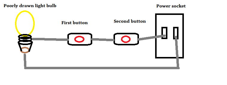
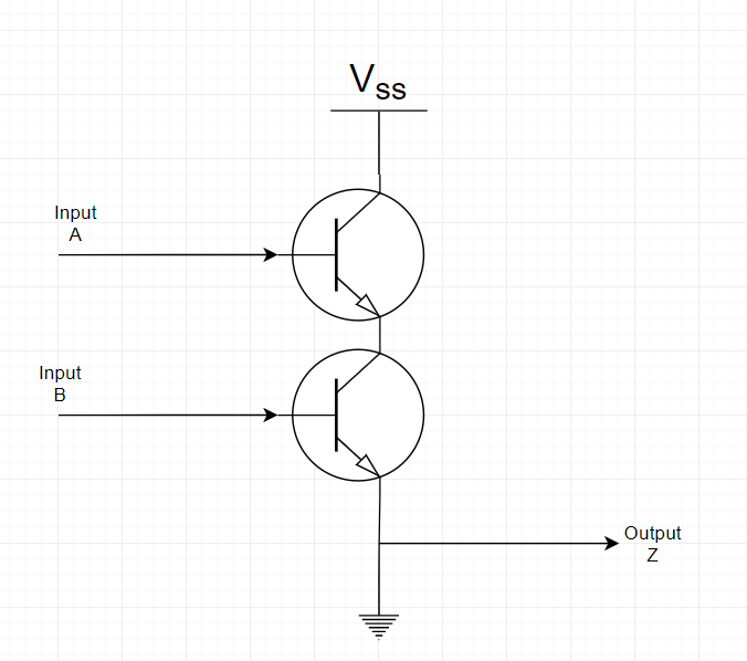
Let’s see how you can create an AND gate using transistors… Don’t forget that these are electrical components, which means they need power, like any of your electrical devices, so truly an AND gate will have 5 entries (known as ‘pins’), one VCC (power), one ground (represents 0V), the A and B inputs and the Z output, you can imagine it as being one box that you plug into your wall power socket, and it has two buttons and one light bulb, if you press both buttons, the light bulb goes on.
So the simple solution would be to connect your light bulb’s ground to the ground pin, and the light bulb’s power connector to one side of the first button, connect the two buttons together and connect the other wire of the second button to the power cord. This way, when you press both buttons, the power flows through the light bulb since the connection is made.. Let me show you my awesome skills in using Paint :
Thinking about it in terms of transistors, you would connect the Z output to one end of a transistor, connect the other end to one end of another transistor, and connect that other end to the power, then you can connect your A input to the ‘S’ pin of one transistor, and your B input to the ‘S’ pin of the second transistor… Here’s what a properly drawn (just means I didn’t use Paint this time, but it’s still a simplification) electrical schema would look like :
I will leave it to you as an exercise to try and figure out how to connect transistors together in order to create an OR, XOR and NOT gate.
Now, that’s about as far as I got when writing this in 2013, and I don’t remember all I had planned to write, but I think that the following section is going to be interesting.. it was one of the most interesting things I had to do at university. I won’t use blue for the rest, but whatever is written below was written in 2019.
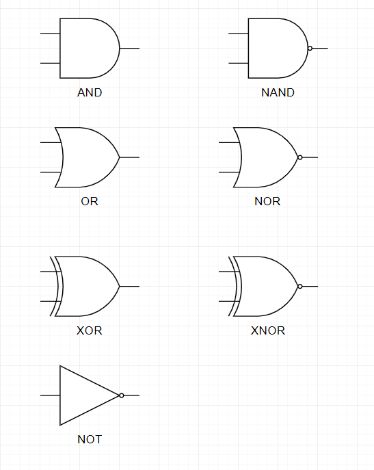
One last thing I want to say about logic gates before we get started is that, this is how they are represented in schematics :
A simple adder
The task we will be doing now is to create a simple adder. An adder is a small electrical circuit which does an addition and nothing else. A simple adder is the same thing but it only does it for single digit numbers (which means a single bit, in the binary world). Get ready, we’re gong to kick it up a notch…
The first step will be to create the Truth Table for our adder. If we add 0 + 0, that gives us 0, that’s obvious.. if we add 1 + 0 that gives us 1, same thing for 0 + 1 of course, but then what do we do with 1 + 1 ? That gives us 10 (which is 2 in binary), but we’re working with a single bit, so ? So it’s simple, the answer is 0 and we have a carry.
Here’s the truth table for our adder which takes two inputs A and B and gives the sum S as its output :
| A | B | S |
| 0 | 0 | 0 |
| 0 | 1 | 1 |
| 1 | 0 | 1 |
| 1 | 1 | 0 |
Does this look familiar? Yes, exactly, it’s the same truth table as the XOR table above… So a simple XOR logic gate is already doing an addition for us!
Let’s make it a little more complicated, what if our adder had two outputs, the sum S and the carry value C. We get this truth table :
| A (Input) | B (Input) | C (Output) | S (Output) |
| 0 | 0 | 0 | 0 |
| 0 | 1 | 0 | 1 |
| 1 | 0 | 0 | 1 |
| 1 | 1 | 1 | 0 |
If we just look at the C column, it looks very similar to the truth table of the AND gate.. So the Carry bit is the result of an AND gate. That sounds really simple, let’s create a circuit with that :
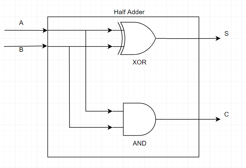
That looks simple enough, right? Well, it is, but it’s also pretty useless, right? What can you do with just 1 bit additions… Also, the one with the most observation, may have noticed that the circuit above was titled ‘Half adder’ and wondering what I mean by ‘half adder’.. well, it just means that it doesn’t take into account a possible carry from a previous operation. A full adder will be the same thing, but it also takes a third input ‘CIN’ (for Carry-In) to do the addition.
If we were to do a full adder, we’d need 3 inputs, and here is the truth table for it (try to write it yourselves before looking, would be interesting to see if you get it right) :
| A (Input) | B (Input) | CIN (Input) | COUT (Output) | S (Output) |
| 0 | 0 | 0 | 0 | 0 |
| 0 | 0 | 1 | 0 | 1 |
| 0 | 1 | 0 | 0 | 1 |
| 0 | 1 | 1 | 1 | 0 |
| 1 | 0 | 0 | 0 | 1 |
| 1 | 0 | 1 | 1 | 0 |
| 1 | 1 | 0 | 1 | 0 |
| 1 | 1 | 1 | 1 | 1 |
Do you want to try and figure out what logic gates to use to build such a circuit ? There are equations you can use to determine the most optimal gates for each output based on the inputs and the truth table, but I’m not going to show you that here. Instead if you filled the table yourself or looked at it enough to understand it, or just use your brain’s logic, you would have figured out that a full adder is basically just doing the sum of the 3 inputs, so it’s a 3 bit addition, so ‘A + B + CIN’ or ‘(A + B) + CIN’, yes.. it can be built using two half adder. Let’s do that now :
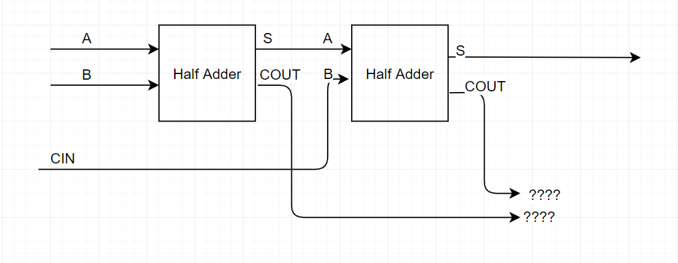
Well.. we have a problem, once we add the partial sum S from the first half adder and add the carry CIN to it, we end up with two carry values, one from each half adder, plus our sum. Are we back to square one having to add 3 bits again? How do we determine our own sum and carry output? Well, let’s do a truth table using the partial sum S1 and carry C1 with the second operation’s sum S2 and carry C2.
Note that we know that the sum value S1 will always be 0 if C1 is 1, and S2 will always be 0 if C2 is 1 (see the half adder’s truth table above). But also that the carry C2 can never be 1 if both CIN and S1 are not 1. Therefore, we can only put a 1 in the C2 column if S1 is also 1, and we can only put 1 on the S1 or S2 columns if C1 or C2 respectively are 0. We also know that if S1 is 1, then we can’t have both S2 and C2 set to 0.
| A (Input) | B (Input) | CIN (Input) | S1 | C1 | S2 | C2 | COUT (Output) | S (Output) |
| 0 | 0 | 0 | 0 | 0 | 0 | 0 | 0 | 0 |
| 0 | 0 | 1 | 0 | 0 | 1 | 0 | 0 | 1 |
| 1 | 1 | 0 | 0 | 1 | 0 | 0 | 1 | 0 |
| 1 | 1 | 1 | 0 | 1 | 1 | 0 | 1 | 1 |
| 1 0 | 0 1 | 1 1 | 1 | 0 | 0 | 1 | 1 | 0 |
| 1 0 | 0 1 | 0 0 | 1 | 0 | 1 | 0 | 0 | 1 |
Looking at the table, we can see that our output S is always the same value as S2, and that our carry COUT is 1 if any of the two operations caused a carry, in other words, if we clear out the columns we don’t care about in the previous table, it’s looking like this :
| C1 | C2 | COUT |
| 0 | 0 | 0 |
| 1 | 0 | 1 |
| 0 | 1 | 1 |
That looks like a simple OR gate, so let’s do that and we get our full adder :
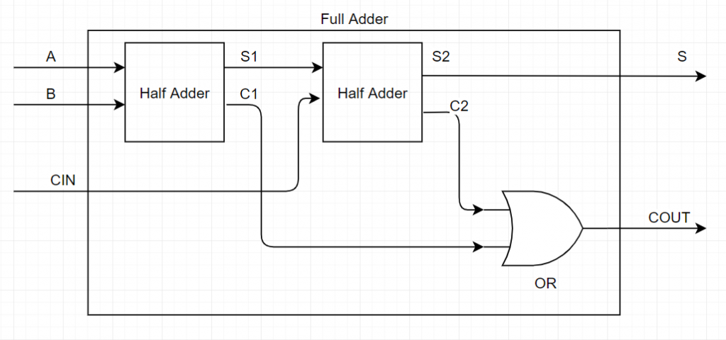
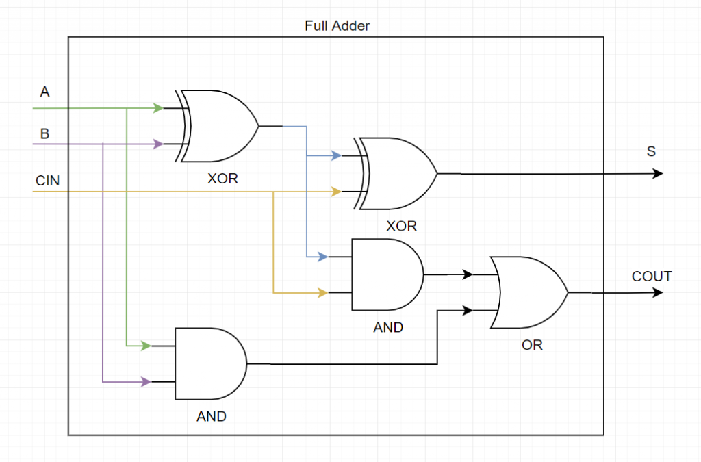
Or if we ignore the half adder blocks and just show the logic gates in use, this is the result :
So, you know how to do additions using logic circuits and you’re probably wondering how that’s useful and how that helps you better understand how a computer works. Well, the reason the full adder is so cool is that you can chain it up. So here’s a very simple 4 bit adder :
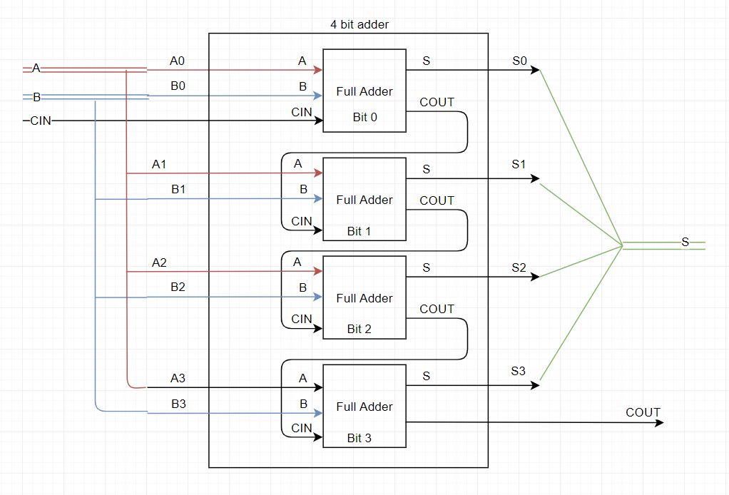
It’s not so bad, right? you have a 4 bit value (0 to 15) A and another 4 bit value B, you can add it and get your sum S on 4 bits with a carry. You can do this until you get to 32 bits, which is a full integer on 32 bit systems.
By having a 32 bit adder, and a substracter and divider and multiplier and all sorts of other small components like that, using logic gates which use transistors, you end up with a bigger block called the ALU (Arithmetic Logic Unit) and with even more complex circuits, you end up with a CPU (Central Processing Unit) which is what runs your entire computer’s logic.
Multiplexers and demultiplexers
I’m not going to get into multiplexers (mux) and demultiplexers (demux) too much, but I want to explain the basic concept. A multiplexer will select one input based on a selector and put it into its output. Let’s assume we have 8 input lines, I0, I1, I2, … I7, and one output Z.. we want to connect Z to one of those input lines, so we use a 8-to-1 multiplexer and use a 3 bit selector (since 3 bits can hold values 000b (0 in decimal) to 111b (7 in decimal) which is enough for our 8 inputs). Based on the value of the selector, the output will be connected to the appropriate input. Sounds simple enough right ?
You can read more about them on this wikipedia page and here’s a drawing taken from that page that shows the logic gates used to construct a 4 to 1 mux :

A demuxer is the opposite. It receives one input and a selector and outputs it one of its numerous outputs. So let’s say a demuxer has 8 outputs, if the selector has value 5, then the 5th output will be connected with the input of the demuxer.
Why I’m explaining all of this? Because the computer is a big muxer/demuxer and that’s how it executes code. You remember when I said that a transistor actually has 5 pins? the 2 inputs A and B, the output Z but also a power input and a ground input to actually power it ? Well, since logic gates are made of transistors, they also need to be connected to both a power source and ground (how would you expect a NOT to output a 1 (which is 5 Volts) if it receives 0 as inputs (which is 0 volts).. we’re not creating energy out of thin air! So yes, these circuit diagrams are always simplified, but you can always assume that every transistor, every logic gate, and every half/full-adder block, multiplier block, ALU, CPU, etc.. will have a 5V power and ground pin going into it.
Your CPU (or ALU in the example below) receives an instruction and needs to ‘decide’ what to do, so here’s how it does it :
- Connect all your inputs to every instruction block you have, so your A and B inputs will go into the addition block, substraction block, multiplication block, etc…
- At the output, use a gigantic OR gate (chaining multiple OR gates one to the other) to OR the output of all of your instruction blocks and put that as your single output.
- Use a demuxer where the instruction you received is the selector of the demuxer, the input is connected to the 5V power input and each output of the demuxer is connected to the 5V power input of each of your blocks.
- When you receive an instruction, only one of the blocks will be active because only one of those blocks will receive power.
And that’s how you make your CPU decide on what to do when it receives an instruction 🙂
SR Latch
This is mostly just for fun, but if you’re wondering what else can be done with transistors and logic gates, how about memory ? Yes, a simple 1 bit memory component can be created using a few logic gates, they are called flip flops. A simple one is called an SR Latch. the ‘SR’ is because of its inputs. S for ‘set’ (set the memory value to 1) and ‘R’ for Reset (set the memory value to 0). Can you figure out how to create a small block with only two logic gates which can act as memory ? Here’s a hint, you only need 2 NORs… how would you connect them in such a way that it remembers the last value you set/reset it to ?
Well, you can read more about flip flops on wikipedia here and here’s how it can be done :
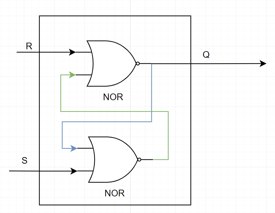
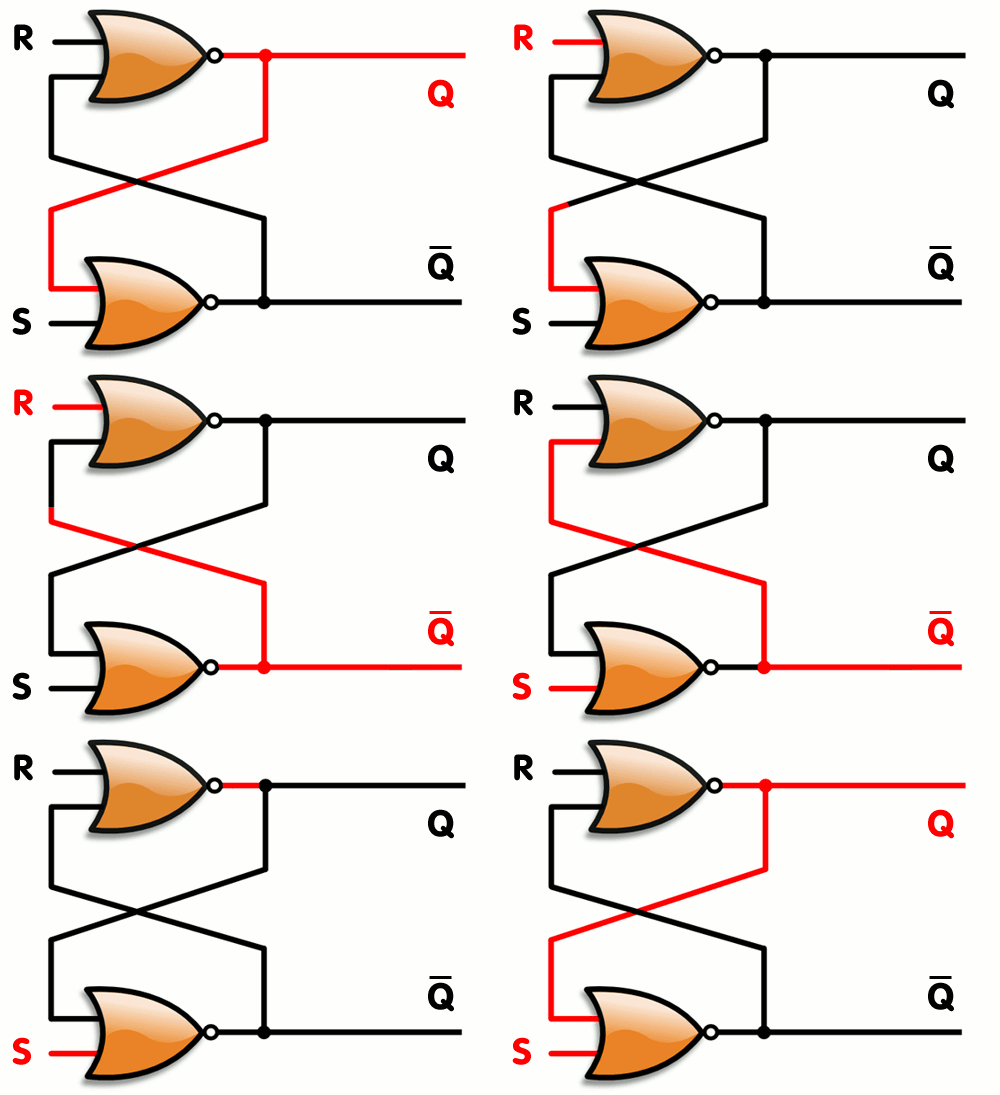
As you can see, by connecting the two gates’s output as input to their companion, you create memory.. Once you set 1 to the S value, the bottom NOR gate will output a 0, which will cause the top gate to output a 1 (remember, a NOR will like an OR gate with a NOT at the end, so it will output a 0 whenever an input is 1 and will output 1 when both inputs are 0). When the top gate is outputting 1, this causes the bottom gate to keep receiving a 1 on its inputs even if S stops being set. When setting R to 1, it will force the top gate to output 0, which does the same thing in reverse… Here’s a simple animation that shows how it works (copied from its wikipedia article) :
Conclusion
You can build from that, from the simple “electricity means 1 and no electricity means 0”, into using transistors (basically electric push buttons) to build the AND, OR, NOT, XOR logic gates to building a more complex logical block such as an adder or a demuxer to building an even more complex processing unit such as an ALU using multiple blocks and a demuxer to interpret instructions it receives to building the extremely complex CPU which handles billions of instructions per second in order to do what we want it to do.
The transistors let us create memory, and computers and basically any electronics device will have transistors in them. According to the wikipedia page for transistor count, a recent CPU has about 7 billion transistors. The iPhone 11 Pro has 8.5 billion, and the PS3’s Cell processor had 250 million transistors… And to think that at some point in the past, a single transistor was as big as a light bulb…
I hope this was interesting and entertaining and mostly educational. I’ve obviously gone very quickly from the very basic to the very complex, but I hope you were all able to follow regardless and even if you don’t understand all of it, you get the broad strokes and understand better how a computer works.
